| |
|
 Oxygen Plasma Etching and Treatment Oxygen Plasma Etching and Treatment
|
Sample cleaning for SEM, TEM, FIB
|
Photoresist ashing, descum, MEMS
|
|
산소 플라즈마 에칭, 표면 처리
|
SEM, TEM, FIB 샘플 클리닝
|
포토레지스트 에싱, 디스컴, MEMS
|
|
Microfluidic PDMS, glass slide, lab-on-chip
|
Wire bonding/flipchip/underfill/encapsulation
|
Next generation of lithography system
|
|
마이크로플루이딕, PDMS, 유리슬라이드, 랩온 칩
|
와이어 본딩, 플립 칩, 언더필/다이본딩, 인캡슐레이션
|
차세대 리소그래피(NGLs) 장치
|
|
Metal to metal, or composite bonding
|
Plasma treatment for polymer
|
Thin film deposition, surface analysis
|
|
금속-금속, 복합소재 본딩
|
폴리머 플라즈마 처리
|
박막 증착, 표면 분석
|
|
Semiconductor inspection/review/metrology
|
Contamination removal on XPS/SIMS/AES
|
|
|
반도체 검사, 리뷰, 계측
|
XPS, SIMS, AES의 오염 제거
|
|
| |
|
|
실리콘 웨이퍼의 포토레지스트 박리, 디스컴, 유기 오염원 제거
|
Typical applications
- Dry ashing of photoresist
- Descum after paternning
- Clean organic contamination on wafer
- Increase surface hydrophilicity for MEMS device
- Improve bonding strength for wire bonding step
|
Related products - 관련 제품
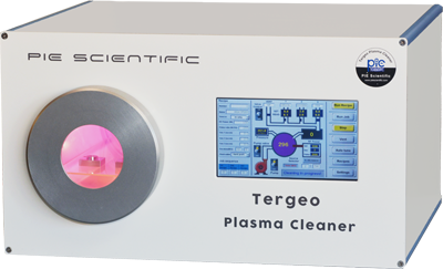 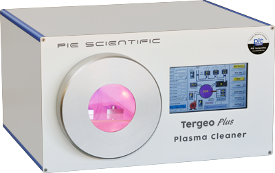
Tergeo and Tergeo-plus tabletop plasma cleaner
건식 포토레지스트 스트립핑, 에싱(dry photoresist stripping, ashing)은 실리콘 웨이퍼의 포토레지스트 층에 급속 케미컬 에칭 공정을
의미합니다. 플라즈마 내의 강력한 전자는 산소 분자를 분해하고 반응성 산소 원자를 생성합니다. 산소 라디칼(Oxygen radicals)은
포토레지스트를 산화시키고 높은 증기압의 일산화탄소, 이산화탄소, 물 등의 부산물을 생성합니다. 소량의 CF4 또는 SF6 가스 첨가는
반응성이 매우 높은 불소 원자가 포토레지스트 폴리머로부터 수소의 추출율을 높여주어 포토레지스트의 에칭 속도를 빠르게 합니다.
포토레지스트 디스컴(Photoresist descum)은 포토레지스트의 패턴과 현상 후의 추가적인 미세한 포토레지스트 에칭 공정입니다.
현상된 곳의 잔여 포토레지스트 찌꺼기를 제거하는데 사용됩니다. 이러한 잔여물은 이후의 건식.습식 에칭 단계를 방해하고 웨이퍼의
균일한 에칭율에 악영향을 줍니다. 디스컴 단계는 포토 마스크 사이드 월 프로파일(side wall profile)을 향상시키고 공정 균일성을
높여줍니다.
실리콘 또는 석영 웨이퍼의 MEMS 디바이스 제조에서 웨이퍼 표면의 유기 오염은 웨이퍼의 접촉각을 높이고 표면을 소수성으로
만듭니다. 또한 와이어 본딩 공정 전 본딩 패드의 유기물 오염원을 제거가 중요합니다.
전통적인 침전 모드 플라즈마 에칭에서 샘플 표면은 중성 라디칼의 화학적 반응과 강력한 이온에 의한 물리적 충격의 대상이 됩니다.
박막 코팅된 디바이스 또는 표면 전하 와 높은 전류네 민감한 디바이스는 플라즈마 세정이 디바이스에 돌이킬 수 없는 손상을 줄 수
있습니다. 이러한 디바이스에는 자유 이온 하향식 모드 플라즈마 클리닝을 추천합니다.
Tergeo 플라즈마 클리너의 경쟁제품 대비 장점
보다 균일한 플라즈마 성능을 나타냅니다. PIE Scientific사는 집중적인 연구를 통해 플라즈마 발생기의 균일도를 향상시켜
왔습니다. 일부 저가의 플라즈마 클리너는 외부 인덕터 코일 타입 안테나를 사용하여 균일한 RF 전기장을 가지기 어렵습니다.
만약 RF 금속 전극이 플라즈마 챔버 내에 위치하면, 내재적인 대칭 구조를 갖지 못합니다. 플라즈마는 고전압의 RF 전극에,
특히 전극 가장자리는, 가까우면 세기가 더 강합니다. Tergeo 플라즈마 클리너는 2개의 대칭적인 외부 전극 디자인으로
다른 플라즈마 클리너 디자인에 비해서 높은 플라즈마 균일성을 가지고 있습니다.
1대의 클리닝 장비에 2가지의 침전 클리닝 모드와 자유 이온 하향식 클리닝 모드를 가지고 있는 Tergeo 플라즈마 클리너는
2개의 플라즈마 소스를 통합한 제품입니다. 디렉트 플라즈마 소스(Direct plasma source)는 전통적인 침전 모드 플라즈마
클리닝에 사용되고, 침전 모드 클리닝에서 샘플은 플라즈마에 침전되는데, 이러한 공정에서는 샘플이 산소 또는 불소 라디칼과
화학적 반응의 대상이 되고 물리적 이온 스퍼터링 충격의 대상이 됩니다. 박막 코팅된 디바이스는 이온 스퍼터링으로 민감한
코팅에 손상을 줄 수 있습니다. 높은 표면 전하 또는 전류는 민감한 IC 디바이스에 손상을 줄 수 있습니다. 이러한 경우에는
하향식 플라즈마 클리닝을 추천하며, 플라즈마는 별도의 원격 플라즈마 소스에서 생성되고, 중성 산소, 불소 라디칼만이 샘플
챔버에 확산되어 포토레지스트와 유기 오염물과 반응을 합니다..
진보된 공정 컨트롤 기술. 플라즈마 균일성과 세기는 챔버 압력에 의해 변화될 수 있습니다. Tergeo 플라즈마 클리너는
진보된 디지털 압력 센서(MEMS MEMS based digital pressure sensor) 기술로 압력 모니터링을 합니다. 또한 PIE Scientific사는
유니크한 플라즈마 센서 기술(unique plasma sensor technology)을 개발하여 실시간 플라즈마 세기를 모니터링 할 수 있습니다.
정량적 데이터는 일상의 반복적이고 이룰적인 결과를 얻는데 중요한 사항입니다.
전자동 오퍼레이션-Fully automatic operation. 몇몇 기초적인 플라즈마 시스템들은 사용자가 플라즈마 챔버 내로의
가스유입에 니들 밸브를 수동으로 조절합니다. 이러한 수동 조절로는 정확한 반복적 그스 유량을 얻기가 불가능합니다.
Tergeo 플라즈마 클리너는 전자동 유량제어기(mass flow controller (MFC)를 사용하여 0에서 to 100sccm꺼지 0.2 sccm 미만의
정확도로 가스 유량을 정밀 제어합니다. 마이크로 컴퓨터가 내장된 저희 장비의 전자동 운영은 다양한 레시피의 일상의
반복적인 작업 수행을 정확하게 할 수 있도록 합니다.
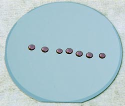 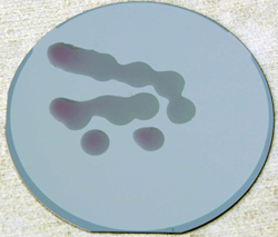
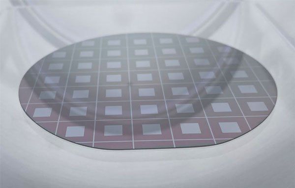
Oxygen plasma treatment to remove organic contamination on wafer surface and increase surface wettability
산소 플라즈마 처리에 의한 웨이퍼 표면의 유기 오염원 제거는 표면 젖음성이 증가합니다.
|
Photoresist ashing or stripping
|
|
|
Photoresist ashing or stripping refers to the process of completely removing the photoresist layer on the substrate. Photoresist stripping can also be achieved through a chemical process. But the wet chemical processes can generate toxic waste. Oxygen plasma photoresist ashing process using radical oxygen to oxidize the organic photoresist. The byproducts are usually COx, H2O gases that are not toxic. The plasma ashing process is also called dry ashing. It’s much more environmentally friendly than the wet chemical stripping process.
|
| |
|
|
| |
|
Electrons in the oxygen plasma can dissociate the oxygen molecules and generate radical monatomic oxygen, which is much more reactive to organic photoresist. Plasmas for the ashing or stripping process are usually generated by MHz (radiofrequency) to GHz (microwave) plasma systems. Adding a minute amount of CF4 or SF6 can significantly increase the ashing speed. Ashing speed can also increase with the temperature of the substrate.
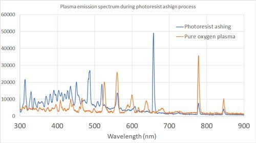
The byproduct generated in the photoresist ashing process can change the plasma emission spectrum. A plasma system equipped with an optical spectrometer can monitor the progress of the photoresist ashing process. As shown in the image below, the plasma emission from CO at 483nm and 520nm and the emission from H at 486nm and 657nm during photoresist ashing is very different from pure oxygen plasma emission. Therefore, it’s possible to monitor the plasma emission from these frequencies to determine the progress of the photoresist ashing process.
|
 |
|
|
|
|
|
Photoresist descum is the process of removing the photoresist residual in the open trenches or holes after the lithography and developing steps. The photoresist residual is usually on the nanometer scale. If the residual is not removed, it can cause a uniformity issue for the subsequent etching process. The residual can also create problems for metal deposition or the electroplating process. The photoresist descum process can be carried out with oxygen plasma in the direct mode or downstream mode. The downstream mode plasma can limit the damage caused by energetic ion sputtering.
Descum process is usually fairly short and runs at a relatively low rf power. So the change of the temperature on the wafer is not significant. Plasma systems used for descum are usually created by radiofrequency or microwave plasma at the frequency ranging from MHz to GHz.
|
| |
|

|
| |
|
|
|
